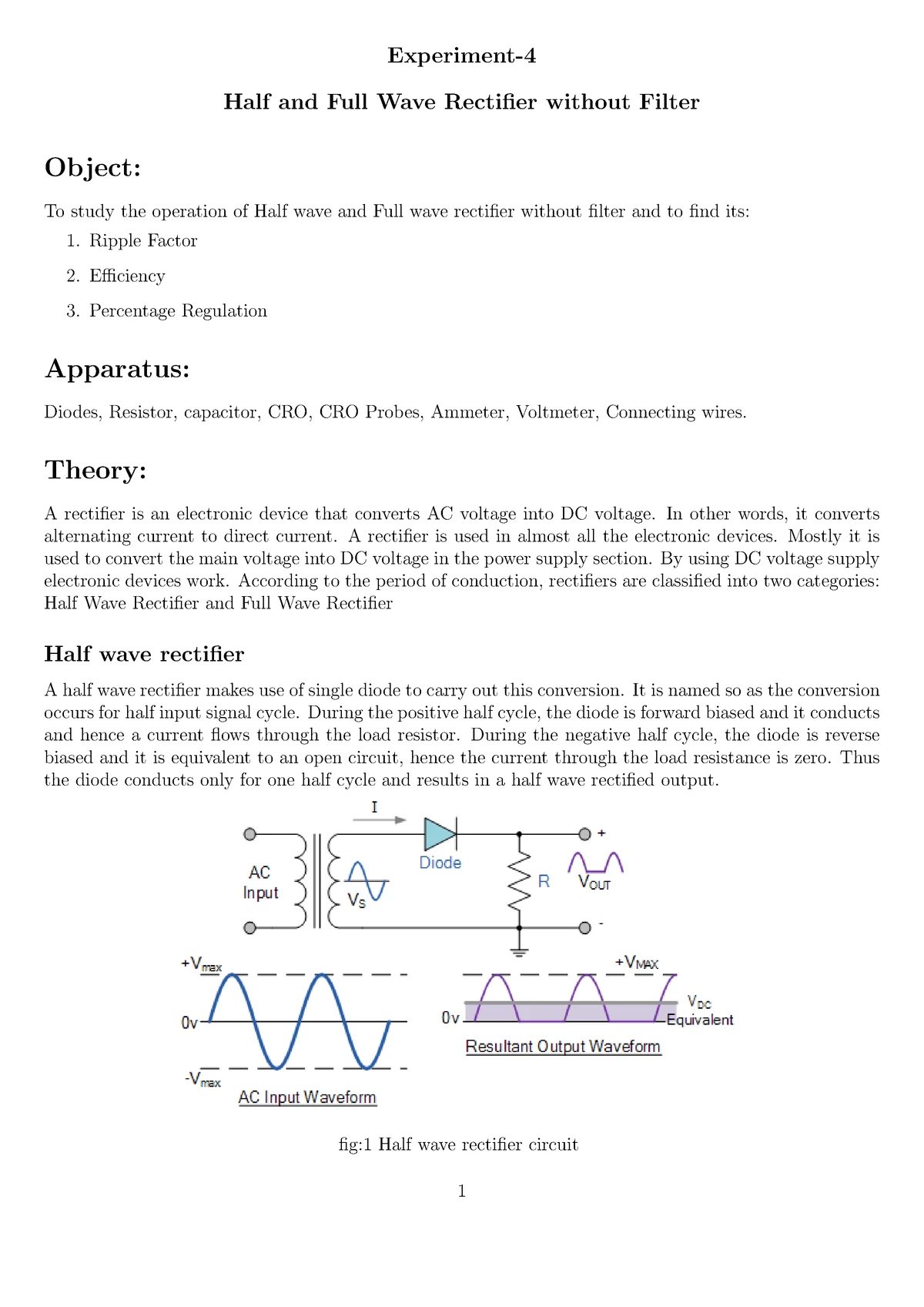
- Physics Practicals
- Physics Viva Questions With Answers
- physics class 12 viva questions with answers
- to draw the i v characteristic curve of a p n junction in forward bias and reverse bias viva questions

To draw the I-V characteristic curve of a p-n junction in forward bias and reverse bias.
1) What are the materials required for this experiment?
A P-N junction diode, 50-volt battery, one 3-volt battery, one 0-3 volt voltmeter, one a high resistance rheostat, one 0-100 μA ammeter, one 0-50 volt voltmeter, one 0-100 mA ammeter, connecting wires, one-way key, and sandpaper are the materials required for this experiment.
2) Give three main precautions that should be taken while doing this experiment.
The connections must be clean, right, and neat. A key must be used while the circuit is active. After the breakdown, voltage (forward bias) must not be provided.
3) What are the three types of materials based on electrical conductivity?
Conductors, insulators, and semiconductors are the three types of materials based on electrical conductivity.
4) What is electrical conductivity?
Electrical conductivity is a measure of how smoothly a body allows current to move through it.
5) What is the relationship between resistivity and electrical conductivity?
The electrical conductivity of the material is reciprocal to resistivity.
6) What is a hole in the context of a semiconductor?
A hole is a place in the crystal lattice of a material which is vacated by an electron. It is considered a positive charge.
7) What is an intrinsic semiconductor?
An intrinsic semiconductor is a pure semiconductor that does not possess any significant dopant species. It is also called an i-type semiconductor or undoped semiconductor.
8) What is an extrinsic semiconductor?
An extrinsic semiconductor is an impure semiconductor that possesses significant dopant species.
9) What is an n-type semiconductor?
An n-type semiconductor is a type of intrinsic semiconductor doped using arsenic (As), antimony (Sb) or phosphorus (P) as an impurity.
10) What is meant by doping?
Doping is the process of deliberately adding appropriate impurities to pure semiconductors.
11) What is meant by a junction?
A junction is a common surface of p-type and n-type semiconductors.
12) What is meant by a junction potential barrier?
A junction potential barrier is a potential difference between junction terminals of semiconductors.
13) What are the two types of biasing?
Forward biasing and reverse biasing are the two types of biasing.
Stay tuned to BYJU’S and Fall in Love with Learning!
- To draw the I-V characteristic curve of a p-n junction in forward bias and reverse bias
- Chapter Wise Physics Class 12 MCQs
- Physics Class 12 Practicals list
Register with BYJU'S & Download Free PDFs
Register with byju's & watch live videos.
- You don't have any recent items yet.
- You don't have any courses yet.
- Add Courses
- You don't have any books yet.
- You don't have any Studylists yet.
1. PN junction
- Multiple Choice
Course : Lab II (PHB21L)
University : jamia millia islamia.

- More from: Lab II PHB21L Jamia Millia Islamia 10 documents Go to course

Recommended for you
Students also viewed.
- Whittlesey Classification
- THE Concept OF Community
- Meaning, Theories and Models of Corporate Governance
- Indifference Curve Analysis
- Social Welfare - Lecture notes 3
- Marketing Management - Assignment April 2022 WJAHaw HQ 7c
Related documents
- Viva-voce-semiconductors
- Meaning, objectives, nature and Scope of Industrial Relations
- Features of Modern Drama in English Literature
- Pandita Ramabai’s views on 'Patriarchy'
- Idea of Bharatvarsha - Lecture notes 2
- The nature and scope of Geomorphology
- About Contact Sing up Log in
- Business & Industries
- Shipping & Logistics
- Markets & Trading
- Finance & Loan
- Automobiles
- Cryptocurrency
- Beauty & Skin Care
- Gift & Jewellery
- Pets & Animals
- Software & Web Development
- Digital Marketing
- Latest Technologies
- Education & Training
- Jobs & Career
- Health & Fitness
- Medical & Health
- Sports & Athletics
V-I Characteristics of p-n-Junction Diode
V-I characteristics of p-n-Junction Diode
Objectives:
- To understand the basic concepts of semiconductors.
- To study p type and n type semiconductor and potential barrier.
- To understand forward and reverse biasing.
- Perform the experiment on bread board and the trainer kit and plot the graph of V-I characteristics of PN junction diode.
Components and equipments required: single strand cable, diode, resistors, bread board, multimeter, connecting wires, CRO, voltage source.
General Instructions: You will plan for Experiment after self study of Theory given below, before entering in the Lab.
PN Junction Diode The effect described in the previous tutorial is achieved without any external voltage being applied to the actual PN junction resulting in the junction being in a state of equilibrium. However, if we were to make electrical connections at the ends of both the N-type and the P-type materials and then connect them to a battery source, an additional energy source now exists to overcome the barrier resulting in free charges being able to cross the depletion region from one side to the other. The behavior of the PN junction with regards to the potential barrier width produces an asymmetrical conducting two terminal device, better known as the Junction Diode.
A diode is one of the simplest semiconductor devices, which has the characteristic of passing current in one direction only. However, unlike a resistor, a diode does not behave linearly with respect to the applied voltage as the diode has an exponential I-V relationship and therefore we cannot described its operation by simply using an equation such as Ohm's law. If a suitable positive voltage (forward bias) is applied between the two ends of the PN junction, it can supply free electrons and holes with the extra energy they require to cross the junction as the width of the depletion layer around the PN junction is decreased. By applying a negative voltage (reverse bias) results in the free charges being pulled away from the junction resulting in the depletion layer width being increased. This has the effect of increasing or decreasing the effective resistance of the junction itself allowing or blocking current flow through the diode.
Then the depletion layer widens with an increase in the application of a reverse voltage and narrows with an increase in the application of a forward voltage. This is due to the differences in the electrical properties on the two sides of the PN junction resulting in physical changes taking place. One of the results produces rectification as seen in the PN junction diodes static I-V (current-voltage) characteristics. Rectification is shown by an asymmetrical current flow when the polarity of bias voltage is altered as shown below.

But before we can use the PN junction as a practical device or as a rectifying device we need to firstly bias the junction, ie connect a voltage potential across it. On the voltage axis above, "Reverse Bias" refers to an external voltage potential which increases the potential barrier. An external voltage which decreases the potential barrier is said to act in the "Forward Bias" direction.
There are two operating regions and three possible "biasing" conditions for the standard Junction Diode and these are:
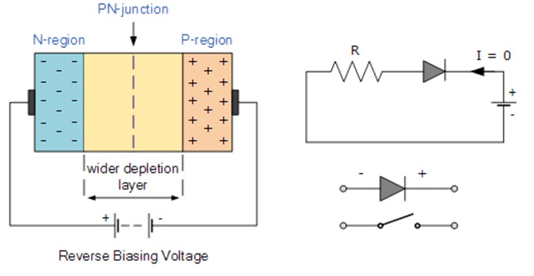
- Reverse Bias - The voltage potential is connected negative, (-ve) to the P-type material and positive, (+ve) to the N-type material across the diode which has the effect of Increasing the PN-junction width.
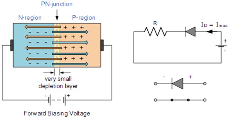
- Forward Bias - The voltage potential is connected positive, (+ve) to the P-type material and negative, (-ve) to the N-type material across the diode which has the effect of Decreasing the PN-junction width.
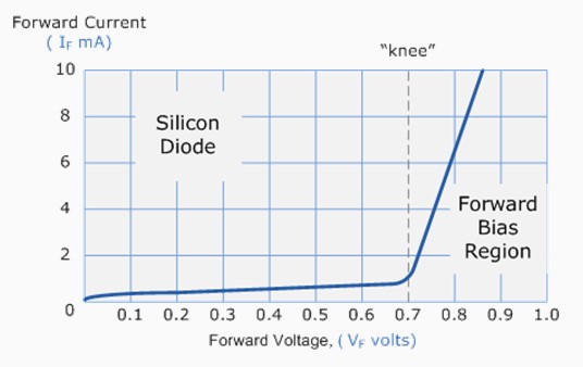
Forward Biased Junction Diode When a diode is connected in a Forward Bias condition, a negative voltage is applied to the N-type material and a positive voltage is applied to the P-type material. If this external voltage becomes greater than the value of the potential barrier, approx. 0.7 volts for silicon and 0.3 volts for germanium, the potential barriers opposition will be overcome and current will start to flow. This is because the negative voltage pushes or repels electrons towards the junction giving them the energy to cross over and combine with the holes being pushed in the opposite direction towards the junction by the positive voltage. This results in a characteristics curve of zero current flowing up to this voltage point, called the "knee" on the static curves and then a high current flow through the diode with little increase in the external voltage as shown below.

The application of a forward biasing voltage on the junction diode results in the depletion layer becoming very thin and narrow which represents a low impedance path through the junction thereby allowing high currents to flow. The point at which this sudden increase in current takes place is represented on the static I-V characteristics curve above as the "knee" point.
This condition represents the low resistance path through the PN junction allowing very large currents to flow through the diode with only a small increase in bias voltage. The actual potential difference across the junction or diode is kept constant by the action of the depletion layer at approximately 0.3v for germanium and approximately 0.7v for silicon junction diodes. Since the diode can conduct "infinite" current above this knee point as it effectively becomes a short circuit, therefore resistors are used in series with the diode to limit its current flow. Exceeding its maximum forward current specification causes the device to dissipate more power in the form of heat than it was designed for resulting in a very quick failure of the device.
Reverse Biased Junction Diode When a diode is connected in a Reverse Bias condition, a positive voltage is applied to the N-type material and a negative voltage is applied to the P-type material. The positive voltage applied to the N-type material attracts electrons towards the positive electrode and away from the junction, while the holes in the P-type end are also attracted away from the junction towards the negative electrode. The net result is that the depletion layer grows wider due to a lack of electrons and holes and presents a high impedance path, almost an insulator. The result is that a high potential barrier is created thus preventing current from flowing through the semiconductor material.
Procedure:-
- Make the connections as shown in fig.:
- Switch on the power supply.
- Now vary in small step the forward bias voltage and current readings on multimeter. Draw the graph between current and voltage.
- Make the connection as shown in fig:
Observation:
Forward biasing

Observation Table
Reverse biasing

Do and Don’ts to be strictly observed during experiment:
Do (also go through the General Instructions):
- Before making the connection, identify the components leads, terminal or pins before making the connections.
- Before connecting the power supply to the circuit, measure voltage by voltmeter/multimeter.
- Use sufficiently long connecting wires, rather than joining two or three small ones.
- The circuit should be switched off before changing any connection.
- Avoid loose connections and short circuits on the bread board.
- Do not exceed the voltage while taking the readings.
- Any live terminal shouldn't be touched while supply is on.
Outputs: Submit the graph as per observation table.
Latest Post

Top 8 Female Casino Streamers Making Waves in 2024

Kirill Yurovskiy: How to Calculate Travel Time

Mastering Pool Cleaning Robot Safety and Efficiency: Your Essential Guide


E-Sports and Betting: The Perfect Match for the Digital Age

Timur Turlov: Visionary Entrepreneur and Advocate for Financial Innovation

How to Use Futures and Options for Hedging Strategies

Freedom Holding Corp: A Leader in the Global Financial Market
Related categories.
- Instrumentation & Measurement
- Analog & Digital Communication
- Analog Electronics
- Digital Electronics
- Electronic Devices & Circuits
- Digital Circuit System
- Digital Communication
- Electronic Circuit Design
- Microprocessor & Interfacing
- Electrical Machines 1
- Electrical Machines 2
- Power Electronics
Electronic Devices & Circuits Lab Experiment list
- 1 Experiment to Study Half Wave vs Full Wave Rectifier
- 2 Study Input vs Output Characteristics of Transistor in Common Emitter Configuration
- 3 Experiment to Study V-I characteristics of Zener Diode.
- 4 To observe front panel control knobs vs to find amplitude, time period vs frequency for given waveforms.
- 5 To Study Characteristics of FET Transistor
- 6 V-I Characteristics of p-n-Junction Diode
- 7 Experiment to Study the Characteristics of Uni Junction Transistor
Laboratory Experiment Categories
- Electrical and Electronics
- Civil Engineering
- Engineering Mechanics
- Mechanical Engineering
- Biomedical Engineering
Get all latest content delivered to your email a few times a month.
- Physics Class-12th Notes
- Physics Formulas
- Physics Symbol
- Application of Physics
- Class 8 Science
- Class 9 Science
- Class 10 Science
- Class 11 Science
- Class 12 Science
- Class 8 Study Material
- Class 9 Study Material
- Class 10 Study Material
- Class 11 Study Material
- Class 12 Study Material
VI Characteristics of a P-N Junction Diode
Semiconductors is a kind of material that has resistivity and conductivity in between metals and insulators. On the basis of purity semiconductors are of two types: Intrinsic Semiconductors is a kind of pure semiconductor without any significant dopant (impurities) species present. An intrinsic semiconductor is also called an undoped semiconductor and Extrinsic Semiconductors is a kind of semiconductor they are doped with an impurity, it is known as an extrinsic semiconductor.
p-n Junction Diode
Junction generally means the area or point that bounds two different parts, similarly in diodes junction is a boundary of two semiconductor materials i.e. the p-type and the n-type, semiconductor.
The p-side in the p-n junction has a positive side of the semiconductor and it has an excess of holes whereas the n-side has an excess of electrons, therefore, it is the negative side. The p-n junction in semiconductors is developed by the method of doping. adding impurities in a semiconductor is known as doping.
Formation of p-n Junction
Let us understand for an example, consider a thin p-type silicon semiconductor sheet. If we add a small amount of pentavalent impurity(having valency five) to this, a part of the p-type Si will get converted to n-type silicon. This sheet will now contain both regions i.e. p and n-type region and a junction is created between two regions.
- There are two types of processes that follow after the formation of a p-n junction – diffusion and drift. As we know, diffusion is the process that follows the flow of particles from higher concentration to lower concentration, due to difference in the concentration of electrons and holes at the two sides of a junction, the electrons from the n-side diffuse to the p-side and the holes from the p-side diffuse to the n-side. this leads to raise in diffusion current.
- Also, there is an ionized donor is left behind on the n-side, which is an immobile charge this develop when an electron diffuses from the n-side to the p-side. As the result of this process, a layer of positive charge is developed on the n-side of the junction.
- Similarly, An ionized acceptor is left behind in the p-side when a hole goes from the p-side to the n-side, resulting in the formation of a layer of negative charges in the p-side of the junction. This region of negative (-) and positive charge (+) on either side of the junction is termed the depletion region.
- An electric field direction from a positive charge towards the negative charge is developed, Due to this positive charge region on either side of the junction, Due to this electric field, the flow of electrons and holes takes place. This is termed the drift motion. generally, the direction of the drift current is opposite to that of the diffusion current.
Forward Bias

The forward bias of p-n junction
In biasing semiconductor is connected to an external source. when the p-type semiconductor is connected to the positive terminal of the source or battery and negative terminal to the n-type, then this type of junction is said to be forward-biased. In forward bias the direction of built-in electric field near the junction and applied electric field are opposite in direction. this means that the resultant electric field has a magnitude lesser than the built-in electric field. due to this there is less resistivity and therefore depletion region is thinner. In silicon, at the voltage of 0.6 V, the resistance of the depletion region becomes completely negligible.
Reverse Bias

The reverse bias of p-n junction
In the reverse biasing, the n-type is connected to the positive terminal and the p-type is connected to the negative terminal of the battery . In this case, the applied electric field and the built-in electric field are in the same direction and the resultant of electric field has higher magnitude than the built-in electric field creating a more resistive, therefore depletion region is thicker. if the applied voltage becomes larger, then the depletion region becomes more resistive and thicker.
p-n Junction Formula The potential difference created by the electric field in the p-n junction is given by: E o = V T ln [N d N a / n i 2 ] where E o junction voltage at no bias, V T is the thermal voltage at room temperature i.e. 26mv, N d and N a are the concentrations of impurity and n i is intrinsic concentration.
V-I Characteristics of p-n Junction Diode

V-I characteristics of p-n junction diode
- In forward bias condition p-type is connected to positive terminal of battery and the n-type to the negative terminal of the battery, there is a reduction in the potential barrier, in this condition. For germanium diodes, when the voltage is 0.3 V, and for silicone diodes, when the voltage is 0.7 V the potential barriers decrease and there is a flow of current.
- When the diode is in forward bias , as the voltage applied to the diode is overcoming the potential barrier, the current increases slowly and the curve obtained is non-linear. Once the potential barrier is crossed by the diode, the diode behaves normally and the curve rises sharply as further external voltage increases and the curve obtained is linear.
- When the PN junction diode is under reverse bias , this results in an increase in the potential barrier and resistance also increases. Minority carriers are present in the junction which creates reverse saturation current flows in the beginning.
- If the applied voltage increases rapidly, there is increased kinetic energy due to minority charge carriers which affect the majority charges. In this stage the diode breaks down. or the voltage is called breakdown voltage, This may also destroy the diode.
Sample Questions
Question 1: When silicon is doped with indium it leads to which type of semiconductor?
As we know, Valency of Indium is 3 therefore it is Trivalent in nature, when it is doped in Silicon it has majority of holes, that’s why it is of p-type semiconductor.
Question 2: A transistor has a current gain of 30 Ampere. If the collector resistance is 6 kΩ, the input resistance is 1 kΩ, calculate its voltage gain.
Given, R in =1 kΩ and R out = 6k Ω ∴ R gain = R out /R in = 6/1 = 6 Voltage gain = current gain × Resistance gain = 30 × 6 =180
Question 3: Write characteristics of holes.
Following are the characteristics of holes: A hole is equivalent to a positive electric charge. The mobility of a hole as compare to that of an electron is less.
Question 4: Name the kind of biasing which leads the following result:
a) Increase in resistance,
b) Decrease in resistance and
c) Increase in width of the depletion region.
a) In reverse bias resistance increases. b) In forward bias resistance decrease. c) In reverse bias there is increase in the width of depletion region take place.
Question 5: What is the ratio of electrons and holes in the intrinsic semiconductor?
Number of electrons = n e Number of holes = n h In intrinsic semiconductor, n e = n h n e /n h = 1
Question 6: Define the term breakdown voltage of p-n junction.
In reverse bias condition, when the applied voltage increases gradually at a certain point there is increase in reverse current noticed, this is junction breakdown, corresponding applied voltage is known as breakdown voltage of p-n junction diode.
Similar Reads
- School Learning
- School Physics
- Physics-Class-12
Improve your Coding Skills with Practice
What kind of Experience do you want to share?

IMAGES
VIDEO
COMMENTS
The document contains questions and answers related to the practical viva for the semiconductor practical and optics practical portions of Class 12 Physics. Some key topics covered include: - Definition and characteristics of a P-N junction diode and depletion layer - Behavior of diodes in forward and reverse bias - Properties of intrinsic and ...
Q.12. What is junction diode ? Ans. A junction diode is formed when a p-type semiconductor is in intimate contact with n-type semiconductor. Q.13. What is meant by forward bias ? Ans. A pn junction is said to be forward biased when p-region is connected to positive terminal and n-region to the negative terminal of battery. Q.14.
To draw the I-V characteristic curve of a p-n junction in forward bias and reverse bias. 1) What are the materials required for this experiment? A P-N junction diode, 50-volt battery, one 3-volt battery, one 0-3 volt voltmeter, one a high resistance rheostat, one 0-100 μA ammeter, one 0-50 volt voltmeter, one 0-100 mA ammeter, connecting wires ...
Key topics covered include p-n junction formation and operation, semiconductor doping, resistivity effects of temperature, intrinsic and extrinsic semiconductors, and properties of n-type and p-type materials.
The following are some of the frequently asked questions related to PN-Junction: 1. What is the need for doping? 2. How depletion region is formed in the PN junction? 3. What is leakage current? 4. What is break down voltage? 5. What is an ideal diode? How does it differ from a real diode? 6.
Experiment-V-I characteristics of PN junction diode. Object: To study the V-I characteristics of PN junction diode. Apparatus: A p-n junction diode, 30V battery,High resistance rheostat,0-30V voltmeter, 0− 100 mAammeter, 0-100μA ammeter, and connecting wires. Theory: Do you know how PN-Junction was invented?
In this video I explained the viva question and answer for the PN junction diode experiment.Step by step explanation has been given for a clear understanding...
It covers topics such as the static and dynamic resistance of junction diodes, forward and reverse biasing of PN junction diodes, Zener diodes, breakdown voltage, BJT configurations, FET properties, and silicon controlled rectifiers.
V-I characteristics of p-n-Junction Diode. Objectives: To understand the basic concepts of semiconductors. To study p type and n type semiconductor and potential barrier. To understand forward and reverse biasing. Perform the experiment on bread board and the trainer kit and plot the graph of V-I characteristics of PN junction diode.
V-I characteristics of p-n junction diode. In forward bias condition p-type is connected to positive terminal of battery and the n-type to the negative terminal of the battery, there is a reduction in the potential barrier, in this condition.